|
Spectrofon #18
22 марта 1996 |
|
Designer - Some useful improvements for the Spectrum, as well as The original scheme of the ADC. For owners of modems, an article on how to improve communication.

The "DESIGNER" won big
popular with our readers. Flow of materials from the hardware
revision and modernization of various kinds is very great. So
today, however as always - offer several articles about the
"iron" Spectrum and its problems.
(C) Sorokin, Andrei Y.
A LITTLE ABOUT ALL
I want to share with our readers
magazine pretty podnakopit me information about some of the
hardware revision of computers and other interesting things.
The entry of my article, I dedicate, if nobody objects,
closing theme port # 7FFD. But the rest is no less interesting
nym, though, to judge you.
So, I think that the following lines will make absolutely
clear in this, painful for many, the topic.
Axiom: address bus and data processor
z80 neinversnye ie active level of the unit. The port is not
chosen, "Return to Zero several places, and the installation of
bus addresses a specific number that contains zeros in the unit
audited and discharges into all the remaining. For example, the
bit structure of # 7FFD (32765):
A15 A8 A7 A1
01111111 11111101
Here the units can be found in all categories, except for A1
and A15. "Inverse" system port selection was involved,
apparently, to reduce the number of deciphered elements, but it
is quite obvious that without check remaining bits of the 1-th
state, the port will be selected and the numbers xxFD, FD, 0D,
00. This state of affairs clearly not in favor of a new "super
Speccy", in They start to "hang" a large number of game
programs. But the solution to the problem Yet there is (for all
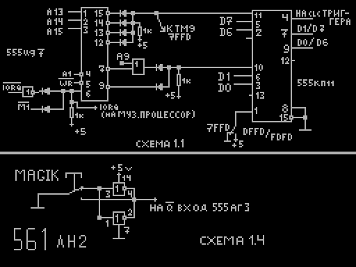
computers except "Scorpion"), a hardware revision
decoding scheme. Basis of the new decoder ms. 555ID7 (see
Figure 1.1)
Differences between my schema of "similar":
1. Soft decoding # 7FFD: on your
PROFI, ATMturbo2 +, ZX (PLA) instantly
will earn a program like "SHOCK"
"EXTERMINATOR", etc.
2. Want to have an ATM and profiles in one (by
dop.pamyati decryption)? No problem, in
"HONEY COMMANDER" f you have enough
memory and built-in HELRa.
In isdos you will el.disk
PROFI512 (1024). Well, you switch s1
translate address ext. port on the main
7FFD (6'7 bit), this mode is used by some boot-s, for example,
"CONVER COMMANDER", because software is much easier manage all
the memory from one port.
3. There is another unused port
# 9FFD "tough" decode.
4. And, of course, both addresses muses. CPU # FFFD '# BFFD,
available as a read and write (on the inactive M1 signal).
Refinement checked on my Speccy-512K,
performed on a single PLA 1515hm1. By the way,
it is to this day - the most compatible platform (do not need
any "silly" improvements such as porta # FF ...). However, PLA
also has some drawbacks-drawbacks!
1. Printed black, with high brightness, a square on a black
background will be bright.
2. Narrow screen.
3. It is impossible (?) Turbocharged processor.
4. For a long (50 cm) loop keyboard buffering is required (it
can also to do and quite often a fault: "failure" keyboard,
when everything else is intact) sm.shemu 1.2.
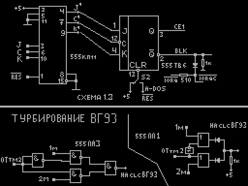
5. In the 128-512kb. reset is very
long, due to the fact that the trigger for 555tv6
resete chooses ROM DOS, the problem is solved
scheme 1.3.
6. Incorrect "MAGIC", to include
ms. 561LN2 on inverted input on 555AG3
antidrebezga scheme, scheme 1.4.
And one more needed in our time completion: disable signal
WG (entry = 0, reading = 1) an additional switch on loop drive,
it will prevent undesirable effects when viewing hakerovskih
works (Kirill Gromov enlighten us, can damage even a well-glued
"Serebryashkoy" disk. See "S" N14).
Now a bit of refinement and flaws
"ATMturbo2 +". Putting the second floor is
one 555id7 + 4 diode (kd522/d9b) + unused piece ms D37 and your
ATM more more "grow" in your eyes, simply "swallow" all sorts
of shocks, strokes and other MEGA (demos). Sm.shemu 1.5.
1. Flaw "turbodvaplyusa: sick scheme
include IBM-keyboards, makes "fail" a lot of programs ("ELITE",
for example). Only one solution - full unsolder controller from
the PROFI.
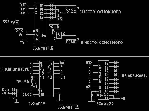
 2. Flaw: invalid INT processor.
3. Flaw: you can not change the recording density
to disk (MFM to FM).
4. Flaw: you can not select 3 and 4 of the drive.
Eliminate the 3 and 4 defects can change TM8
in TM9 in the scheme of the floppy controller.
Now, with your permission, a little
information about the floppy drive controller.
Axiom 2: Any controller has a chain
PLL, and when you begin to "fill up" on
that this controller is better than another
the fact that he has this site, try to evaluate all the
advantages and disadvantages of selected computer.
Axiom 3: the "our" disk.kontrollery not
track ready signal drive
why trouble the owners of 5305 are guaranteed (with
el.magnitom) diskvodov (approximate scheme circumvent this
trouble is in "S" N14. Article K. Gromov).
All controllers should have at the exit
VG93 inventory only 155 series
155LN2 example, 155LN1 - is an order of magnitude
reduce the number of failures in dealing with
floppy. And inside the circuit is better to put
all ms. 555 series, it strongly reduces the current consumption
and increase reliability. 1533 series is better not to put in
any computer, it reduced carrying capacity, at the same as that
of the 555 parameters of the consumption / maks.chastota.
*
(C) Lezhenko Denis (LDE SOFT)
A simple scheme ADC
Before you simple circuit analog-digital converter, which
allows to digitize analog signals from 10 / 8 bit quality.
Despite the simplicity of the scheme, money obtained otsifrovok
comparable quality otsifrovok received on computers IBM / PC or
AMIGA, and often surpasses it.
But what to do with these tsifrovkami? I think today a lot
of talk is not necessary, I remind you only briefly: it is
DIGITAL manufacturer of tools for such well-known music
editors, such as: DIGITAL STUDIO, SAMPLER, INSTRUMENT, DMM
etc. Well, of course, the original design of their programs and
megadem.
But those who understand the word no ADC
only as a toy, capable of recording
music or voice into a computer, provided enormous opportunities
for experimenting with analog signals. For example, using a
simple driver, ADC can be turned into a digital oscilloscope,
frequency counter, voltmeter, multimeter, etc.
Let's move on to describe the connection to the ADC
SPECTRUM'u. To connect I decided to use free ports
AY-3-8910 although you can use any
your existing ports (eg VV55 at
it even simpler software control ADC). Now specifically to the
scheme: for its need to buy to build Mitinskoe radio market and
chip K1113PV1A one (1) resistor. Connects the ADC 15 th
wires (12, 10, 16, 14 - food), 2-9
ADC to the 21-14 AY-3-8910, 17 / D to 7 AY, 1918
ADC to 12 AY, an ADC to 11 AY, ADC 11 to 13
AY. Further, the scheme is clear.
Now it's time to describe the bit-
ports for use with ADC and write your own driver. Port AY "A"
is for receive bytes from the ADC data bus. Port
"B" is designed to receive two younger
ADC bits (you can if you wish not to use), acceptance of the
ADC signal readiness, reset / ADC.
More information about the layout of bits in the port
"B": Bit 0 - quenching / transformation
(0-gashenie/1-preobrazovanie), bit 6 - the willingness ADC
(0-READY) bit 1 - LSB ADC (D0 / D) bit 2 - the first digit of
the ADC (D1). Such a strange layout of bits not
random, it's easier to program the ADC. K
Moreover, treatment of the two LSBs
ADC requires a lot of cycles Z-80, and which
because not enough, so they removed my
a single port and you to decide to use them or not. Personally,
I have them reserved, and I'm quite happy with an 8-
otsifrovok bit quality.
Management Features ADC: Conclusion 15
designed to select the conversion. Let me explain: if the pin
15 logic 0, the ADC operates in a unipolar mode. To switch the
ADC in bipolar mode output 15 should be free. Control signals:
Conclusion 11 / D: suppression / signal conversion. Controlled
bit 0 port "B" AY. Has the following values: 1-quenching,
0-conversion. After receiving the signal ADC starts to convert
the analog signal into digital form by successive
approximation. Therefore, the digital code at the ADC output
comes with a slight delay: about 30mks or about 11 cycles Z-80.
Must take into account this fact, or
poll the ADC signal readiness (17
ADC output, or 6 bits of port "B" AY). When
Logic 0 on this conclusion the ADC is ready
You can shoot bytes on the data bus.
After the ADC generates a signal "ready" should be
considered in bytes of RAM, and then reset the ADC (see above)
and give a signal transformation. Otherwise, the ADC output will
sit old bytes of RAM, and you fill just one digital readout.
Oh, I forgot to remind that, for the ADC should be -15 (or,
at worst, -12) volts, also recalls that in The power supply
voltage from IBM are there.
Technical data of the ADC: the maximum conversion frequency
- 44000 Hz. With the appropriate driver, the conversion time 1
byte: if the signal frequency 50 Hz to 30 ms (10/11 cycles
Z-80). Supply voltage: +5 V, 4 mA,-15V, 15mA.
Input voltage conditions: unipolar
- 0 ... 11V, bipolar: from -5.5 V to 5.5 V.
K 7N / AY
K1113PV1A
K 12n/AY 18 D0 __ 17
K 11n/AY 1 - D1 DR <Login
K 21n/AY 2 D2> 0 <15 R1-4, 7k
K 20n/AY 3 - D3 0VA 14
K 19n/AY 4 - D4 AI 13
K 18n/AY 5 - D5-U2 12 <-15c
K 17n/AY 6 - D6 + U2 10 <+ 5c
K 16n/AY 7 - D7 0VD 16 <Total
K 15n/AY 8 - D8 ___
K 14n/AY 9 - D9 F / P 11
(C) L.D.E. SOFT 1995
K 13n/AY
Well, that's a small description on connecting and
programming the ADC. If who have questions about this, then
contact me at (095)
400-0436 or come to my Mitinskaya radio market (the place of
the X-5), or write address: Moscow, 127572 ul.Novgorodskaya
Building 27, Apt. 55 Lezhenko Denis (LDE SOFT).
*
Next note - for the owners of modems. Perhaps your
communication problems will now be resolved?
Noise Reduction
TELEPHONE LINE USING MODEM
based on the article Mike McCauley
"Modem Noise Killer"
Shown in Figure 1 circuit (3 resistance and capacitor), a
primitive RC-filter that will allow you to reduce the noise of
the telephone line and thereby increase the effective rate of
exchange. Given the variety of operating conditions (different
types of modems, the quality of wiring and PBX equipment, etc.)
in the scheme introduced variable resistors, you can customize
for specific conditions.
The order of the filter settings
- Connect the filter on the proposed scheme.
- Call BBS c which had problems
because of the noise.
- After connecting to estimate the noise level and
performance.
- Try to rotate the axis of variable resistors ("rude" - R1,
"exactly" - R2) and Observe the changes as
communication. By If you do not notice the difference, then
perhaps this is the optimum position.
>>
C1: 1-1.5mkF x 200V
A R1: 10 kOm M
and
Londo
and R2: 2 kOm e
I m
R3: 100 Om x 0.25W
>>
On this today. We will wait for your
new work, designers!
2. Flaw: invalid INT processor.
3. Flaw: you can not change the recording density
to disk (MFM to FM).
4. Flaw: you can not select 3 and 4 of the drive.
Eliminate the 3 and 4 defects can change TM8
in TM9 in the scheme of the floppy controller.
Now, with your permission, a little
information about the floppy drive controller.
Axiom 2: Any controller has a chain
PLL, and when you begin to "fill up" on
that this controller is better than another
the fact that he has this site, try to evaluate all the
advantages and disadvantages of selected computer.
Axiom 3: the "our" disk.kontrollery not
track ready signal drive
why trouble the owners of 5305 are guaranteed (with
el.magnitom) diskvodov (approximate scheme circumvent this
trouble is in "S" N14. Article K. Gromov).
All controllers should have at the exit
VG93 inventory only 155 series
155LN2 example, 155LN1 - is an order of magnitude
reduce the number of failures in dealing with
floppy. And inside the circuit is better to put
all ms. 555 series, it strongly reduces the current consumption
and increase reliability. 1533 series is better not to put in
any computer, it reduced carrying capacity, at the same as that
of the 555 parameters of the consumption / maks.chastota.
*
(C) Lezhenko Denis (LDE SOFT)
A simple scheme ADC
Before you simple circuit analog-digital converter, which
allows to digitize analog signals from 10 / 8 bit quality.
Despite the simplicity of the scheme, money obtained otsifrovok
comparable quality otsifrovok received on computers IBM / PC or
AMIGA, and often surpasses it.
But what to do with these tsifrovkami? I think today a lot
of talk is not necessary, I remind you only briefly: it is
DIGITAL manufacturer of tools for such well-known music
editors, such as: DIGITAL STUDIO, SAMPLER, INSTRUMENT, DMM
etc. Well, of course, the original design of their programs and
megadem.
But those who understand the word no ADC
only as a toy, capable of recording
music or voice into a computer, provided enormous opportunities
for experimenting with analog signals. For example, using a
simple driver, ADC can be turned into a digital oscilloscope,
frequency counter, voltmeter, multimeter, etc.
Let's move on to describe the connection to the ADC
SPECTRUM'u. To connect I decided to use free ports
AY-3-8910 although you can use any
your existing ports (eg VV55 at
it even simpler software control ADC). Now specifically to the
scheme: for its need to buy to build Mitinskoe radio market and
chip K1113PV1A one (1) resistor. Connects the ADC 15 th
wires (12, 10, 16, 14 - food), 2-9
ADC to the 21-14 AY-3-8910, 17 / D to 7 AY, 1918
ADC to 12 AY, an ADC to 11 AY, ADC 11 to 13
AY. Further, the scheme is clear.
Now it's time to describe the bit-
ports for use with ADC and write your own driver. Port AY "A"
is for receive bytes from the ADC data bus. Port
"B" is designed to receive two younger
ADC bits (you can if you wish not to use), acceptance of the
ADC signal readiness, reset / ADC.
More information about the layout of bits in the port
"B": Bit 0 - quenching / transformation
(0-gashenie/1-preobrazovanie), bit 6 - the willingness ADC
(0-READY) bit 1 - LSB ADC (D0 / D) bit 2 - the first digit of
the ADC (D1). Such a strange layout of bits not
random, it's easier to program the ADC. K
Moreover, treatment of the two LSBs
ADC requires a lot of cycles Z-80, and which
because not enough, so they removed my
a single port and you to decide to use them or not. Personally,
I have them reserved, and I'm quite happy with an 8-
otsifrovok bit quality.
Management Features ADC: Conclusion 15
designed to select the conversion. Let me explain: if the pin
15 logic 0, the ADC operates in a unipolar mode. To switch the
ADC in bipolar mode output 15 should be free. Control signals:
Conclusion 11 / D: suppression / signal conversion. Controlled
bit 0 port "B" AY. Has the following values: 1-quenching,
0-conversion. After receiving the signal ADC starts to convert
the analog signal into digital form by successive
approximation. Therefore, the digital code at the ADC output
comes with a slight delay: about 30mks or about 11 cycles Z-80.
Must take into account this fact, or
poll the ADC signal readiness (17
ADC output, or 6 bits of port "B" AY). When
Logic 0 on this conclusion the ADC is ready
You can shoot bytes on the data bus.
After the ADC generates a signal "ready" should be
considered in bytes of RAM, and then reset the ADC (see above)
and give a signal transformation. Otherwise, the ADC output will
sit old bytes of RAM, and you fill just one digital readout.
Oh, I forgot to remind that, for the ADC should be -15 (or,
at worst, -12) volts, also recalls that in The power supply
voltage from IBM are there.
Technical data of the ADC: the maximum conversion frequency
- 44000 Hz. With the appropriate driver, the conversion time 1
byte: if the signal frequency 50 Hz to 30 ms (10/11 cycles
Z-80). Supply voltage: +5 V, 4 mA,-15V, 15mA.
Input voltage conditions: unipolar
- 0 ... 11V, bipolar: from -5.5 V to 5.5 V.
K 7N / AY
K1113PV1A
K 12n/AY 18 D0 __ 17
K 11n/AY 1 - D1 DR <Login
K 21n/AY 2 D2> 0 <15 R1-4, 7k
K 20n/AY 3 - D3 0VA 14
K 19n/AY 4 - D4 AI 13
K 18n/AY 5 - D5-U2 12 <-15c
K 17n/AY 6 - D6 + U2 10 <+ 5c
K 16n/AY 7 - D7 0VD 16 <Total
K 15n/AY 8 - D8 ___
K 14n/AY 9 - D9 F / P 11
(C) L.D.E. SOFT 1995
K 13n/AY
Well, that's a small description on connecting and
programming the ADC. If who have questions about this, then
contact me at (095)
400-0436 or come to my Mitinskaya radio market (the place of
the X-5), or write address: Moscow, 127572 ul.Novgorodskaya
Building 27, Apt. 55 Lezhenko Denis (LDE SOFT).
*
Next note - for the owners of modems. Perhaps your
communication problems will now be resolved?
Noise Reduction
TELEPHONE LINE USING MODEM
based on the article Mike McCauley
"Modem Noise Killer"
Shown in Figure 1 circuit (3 resistance and capacitor), a
primitive RC-filter that will allow you to reduce the noise of
the telephone line and thereby increase the effective rate of
exchange. Given the variety of operating conditions (different
types of modems, the quality of wiring and PBX equipment, etc.)
in the scheme introduced variable resistors, you can customize
for specific conditions.
The order of the filter settings
- Connect the filter on the proposed scheme.
- Call BBS c which had problems
because of the noise.
- After connecting to estimate the noise level and
performance.
- Try to rotate the axis of variable resistors ("rude" - R1,
"exactly" - R2) and Observe the changes as
communication. By If you do not notice the difference, then
perhaps this is the optimum position.
>>
C1: 1-1.5mkF x 200V
A R1: 10 kOm M
and
Londo
and R2: 2 kOm e
I m
R3: 100 Om x 0.25W
>>
On this today. We will wait for your
new work, designers!
Other articles:
|
|
Expertise - the first time in our country is presented and discussed "The Bards Tales "- a full semnadtsatiurovnevaya role-playing game. |
Fantasy - short story on a computer game "Captain Blood". |
Review - the influx of new games: Last Battle, The turn or xor'em all, Tank War, Adventures of Winnie the Pooh War Embera, Open it! |
From the world of bat - post the log and continued discussions about and around Spetrkume him. |
From the world of bat - Hackers and authors are not just people: An Inside Look. |
System - tips for beginning programmers. |
Designer - Some useful improvements for the Spectrum, as well as The original scheme of the ADC. For owners of modems, an article on how to improve communication. |
|
|
Premiere - reclaimed and recycled a demo version of the game "Prince of Persia". |
Advertising - advertising and announcements. |
Similar articles:
В этот день... 30 March